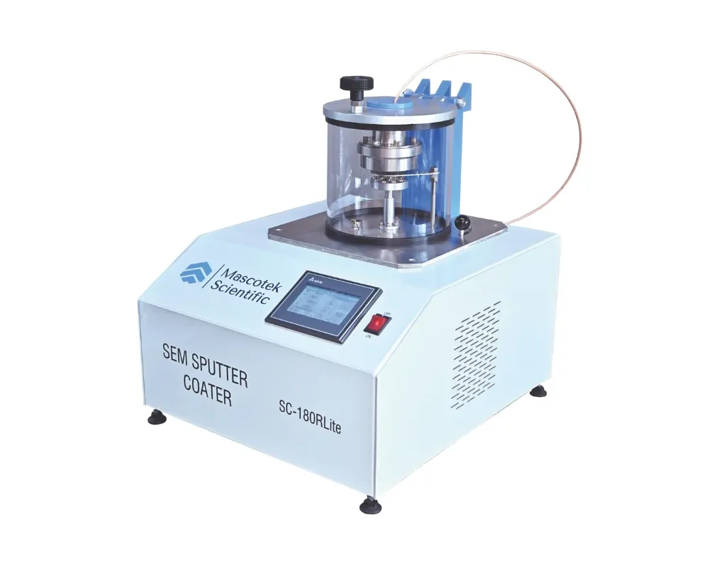
SEM SPUTTER COATER
Other Products
SEM SPUTTER COATER SC 180RLITE

Sputter coating of SEM specimen is the process of coating ultrathin electrically conductive thin films of noble metals like Gold, Gold- Palladium, Platinum, Silver on non-conductive (insulating) specimen. The SC 180RLite is used to coat thin film of gold using atmospheric air or Argon gas as well as thin film of Gold- Palladium alloy, Platinum and Silver using Argon gas. Electrically conductive specimen interact better with the electron beam of the SEM which gives clear image. However non- conductive specimen build up electro static charge from the electron beam of the SEM and therefore interferes with the signal used to create the SEM image. Sputter coating thin fi lms of conductive materials on non- conductive specimens prevents electro- static charge build up over such specimen. It also increases the amount of secondary electrons generated from the specimen surface detected by the SEM which increases the signal to noise ratio resulting in better imaging. Sputtered films for SEM typically range in 2-20
- Chamber: Borosilicate Glass Chamber 120 mm diameter x 120 mm height having Viton Gasket sealing and hinged top flange for easy loading and unloading of specimen and exchange of targets.
- Magnetron Sputter Source: One 57mm diameter Magnetron Sputter source for sputtering of thin films. Magnetron capable of handling 57mm diameter targets. The typical thickness of targets to be sputtered is 0.1mm up to 0.2mm.
- Needle valve: for Air and Argon gas inlet into the chamber.
- Power Supply: Low Voltage power supply to enable current control within 5 mA to 80 mA resulting in controlled deposition of thin films
- Timer: Digital timer to set the sputter time from 5 seconds to 300 seconds
- Specimen Holder to hold max 12 SEM stubs of 12.5 mm diameter. Specimen holder to target distance can be varied between 20mm to 60mm (40mm range adjustment)
- Pumping System: 6 m³/hr rotary pump, suitable to get ultimate vacuum better than 2 x 10⁻²mbar
- Vacuum gauge: Pirani gauge to measure pressure from atmosphere up to 1x10⁻³ mbar
- Cabinet & Controller: Controller is located in one single table top cabinet with necessary safety Interlocks for ‘User Friendly’ operation
- PLC with 4” touch screen HMI
230VAC, 50 Hz
L 367mm X W 450mm x H 400mm

